
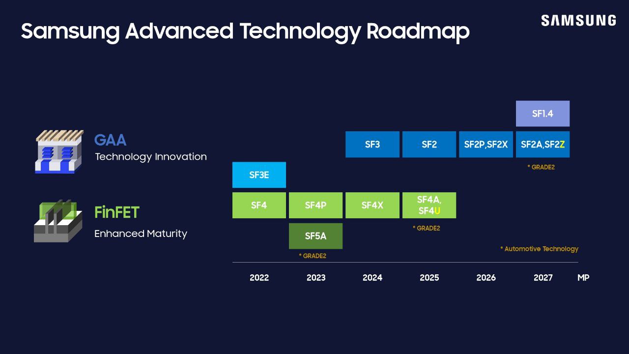
Samsung this week has unveiled its latest process technologies roadmap at the company’s Samsung Foundry Forum (SFF) U.S. The new plan covers the evolution of Samsung’s 2nm-class production nodes through 2027, including a process technology with a backside power delivery, re-emphasizing plans to bring out a 1.4nm-class node in 2027, and the introduction of a ‘high value’ 4nm-class manufacturing tech.
Samsung Foundry’s key announcements for today are clearly focused on the its 2nm-class process technologies, which are set to enter production in 2025 and will span to 2027, when the company’s 1.4-nm class production node is set to enter the scene. Samsung is also adding (or rather, renaming) another 2nm-class node to their roadmap with SF2, which was previously disclosed by Samsung as SF3P and aimed at high-performance devices.
“We have refined and improved the SF3P, resulting in what we now refer to as SF2,” a Samsung spokesperson told AnandTech. “This enhanced node incorporates various process design improvements, delivering notable power, performance, and area (PPA) benefits.”
| Samsung Foundry for Leading-Edge Nodes Announced on June 12, 2024 Compiled by AnandTech | ||||||
| HVM Start | 2023 | 2024 | 2025 | 2026 | 2027 | 2027 |
| Process | SF3E | SF3 | SF2 (aka SF3P) | SF2P/SF2X | SF2Z | SF1.4 |
| FET | GAAFET | |||||
| Power Delivery | Frontside | Backside (BSPDN) | ? | |||
| EUV | 0.33 NA EUV | ? | ? | ? | ? |
This is another example of a rebranding of leading-edge fabrication nodes in the recent years by a major chipmaker. Samsung Foundry is not disclosing any specific PPA improvements SF3P has over SF2, and for now is only stating in high-level terms that it will be a better-performing node than the planned SF3P.
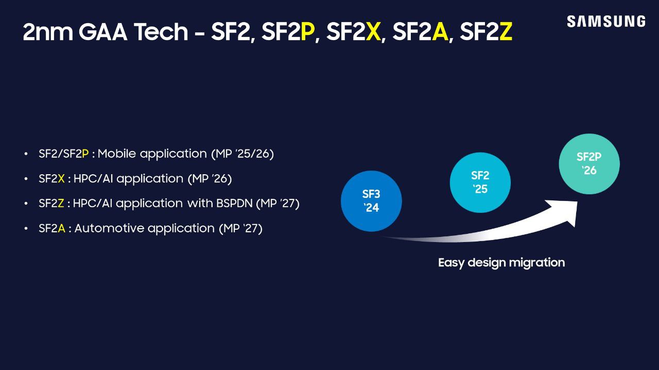
Meanwhile, this week’s announcement also includes new information on Samsung’s next batch of process nodes, which are planned for 2026 and 2027. In 2026 Samsung will have SF2P, a further refinement of SF2 which incorporates ‘faster’ yet less dense transistors. That will be followed up in 2027 with SF2Z, which adds backside power delivery to the mix for better and higher quality power delivery. In particular, Samsung is targetting voltate drop (aka IR drop) here, which is an ongoing concern in chip design.
Finally, SF1.4, a 1.4nm-class node, is on track for 2027 as well. Interestingly, however, it looks like it does not feature a backside power delivery. Which, per current roadmaps, would have Samsung as the only foundry not using BSPDN for their first 1.4nm/14Å-class node.
“We have optimized BSPDN and incorporated it for the first time in the SF2Z node we announced today,” the spokesperson told us. “We will continue to refine this technology and apply it to future nodes, but we don’t have a specific timeline to share at this time.”
| Chip Fab Roadmaps for Leading-Edge Nodes Data announced during conference calls, events, press briefings and press releases. Compiled by AnandTech | ||||||
| HVM Start | 2023 | 2024 | 2025 | 2026 | 2027 | |
| Intel | Process | Intel 3 | Intel 20A | Intel 18A | Intel 14A | Intel 10A |
| FET | FinFET | RibbonFET (GAAFET) | ||||
| Power | Frontside | PowerVia (BSPDN) | ||||
| EUV | 0.33 NA EUV | 0.55 NA EUV + DSA | ||||
| Samsung | Process | SF3E | SF3 | SF2 | SF2P/SF2X | SF2Z/SF1.4 |
| FET | GAAFET | |||||
| Power | Frontside | Backside/? | ||||
| EUV | 0.33 NA EUV | ? | ? | ? | ||
| TSMC | Process | N3E/N3P | N3S/N3X | N2 | A16 | A14 (?) |
| FET | FinFET | GAAFET | ||||
| Power | Frontside | Super Power Rail (BSPDN) | ||||
| EUV | 0.33 NA EUV | ? |
When compared to other contract fabs, Samsung’s roadmap is now roughly in line with the rest in regards to ‘nanometer’ designations. Though absent further technical disclosures from Samsung, it remains unclear what the actual benefits will be for each node and how they compare to their predecessors, let alone how they’ll compare to Intel Foundry and TSMC.


